Key takeaways:
- Semiconductors are key to a sustainable, smart, connected and digital future.
- The semis industry is experiencing strong growth. Its environmental footprint may expand beyond simple capacity growth, as 3D structures and smaller node sizes require extra process steps, novel materials and techniques.
- Wider ecosystem development is needed to lower the environmental footprint and encourage circular processes. Active management, including company engagement can encourage sustainable industry development and identify key winners in the space.
| The JH Explorer series follows our investment teams across the globe and shares their on-the-ground research at a country and company level. |
I recently returned from a European tour of semiconductor manufacturers, an all-important technology sector that is enabling generative AI, which is still very much in its infancy, with an ever-increasing number of use cases and solutions leveraging its capabilities. Being able to see the machines at work, and being on-the-ground, meeting with people always proves invaluable to gain and share additional insight is imperative to navigating this dynamic, highly competitive space.
Semiconductors play a key role in a sustainable future
Semis have revolutionised the world and are enabling breakthrough technologies like generative AI, which has the capability to solve some of the world’s biggest challenges. These capabilities range from modelling physical climate risk, tracking supply chains and identifying corruption or waste, modelling genomes and identifying new medicines, to enabling sustainable transport through providing the compute power for electrification and enhanced safety features. Crucially, the tiny chips also provide the compute power behind data centres, the backbone of our digital society. Therefore unsurprisingly, the semiconductor industry is growing strongly, with revenues forecast to surpass US$1trn by 2030, according to consultancy firm, McKinsey.
Demand for more advanced chips is increasing sustainability challenges
The need for ever-increasing processing power, connectivity and intelligence is driving the shift to chips made from silicon to a diverse range of novel materials, one being silicon carbide (SiC), notably in electric vehicles, renewable energy and industrial applications. Focusing on semis, the improvement in chip performance comes with a downside. SiC chip production can potentially treble CO2 emissions compared to silicon wafers, as the process requires higher temperatures and tougher chemicals, as well as more time, at lower efficiencies.
There is also the drive to reduce feature size (ie. size of the individual components or transistors on a microchip) because as the feature size decreases, more transistors that can be placed on a single chip, enables increased processing power and efficiency. The shift to smaller node size and 3D structures complicates the sustainability journey for semi manufacturers. While it can reduce the amount of wafer needed, it can also lead to an increase in process steps, energy and water consumption, as well as hazardous chemical usage and waste production.
Not taking ESG ratings at face value – insight and engagement invaluable
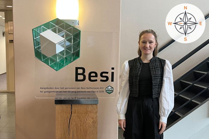
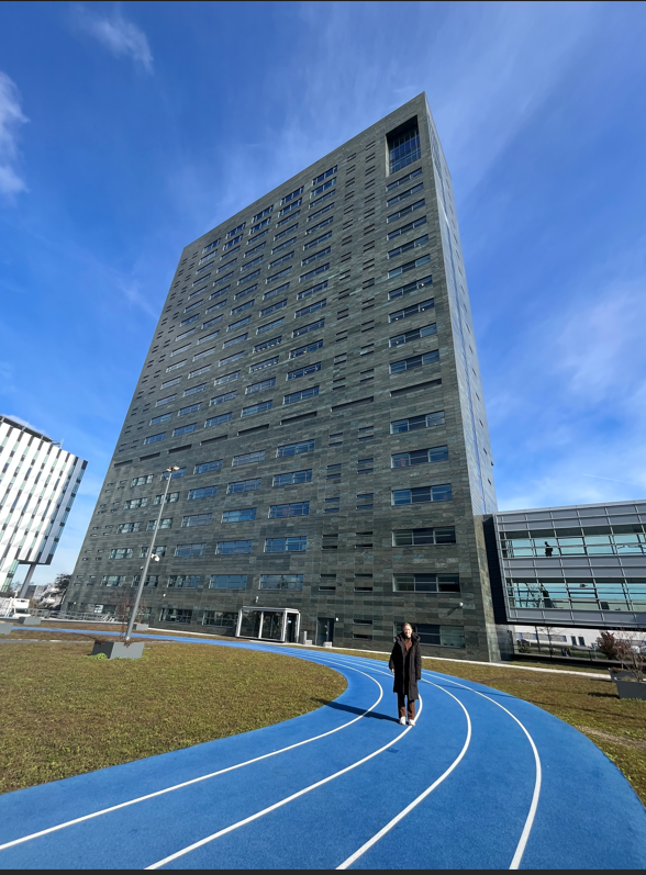
On my trip, some of the places I travelled to included Veldhoven, in southern Netherlands, to visit ASML, a global leader in the designing and manufacturing of lithography machines, an essential component in microchip manufacturing and one of the most energy intense parts of the process. Essentially lithography machines project complex patterns of transistors, layer by layer, on a silicon wafer. I also paid a visit to ASM International in Almere, which supplies wafer processing equipment to semi manufacturers, as well as Duivan in the east to stop by semi equipment maker, Besi.
3D image of an ASML lithography machine

One of the focuses for my trip was to assess the companies from an ESG (Environmental, Social and Governance perspective. In particular I was interested in their wider environmental footprint, i.e. their Scope 3 emissions – not just in terms of carbon, but also water, waste, resources and pollution, as well as checking out their ESG and sustainability efforts firsthand.
While ASML has been awarded the highest rating – AAA by MSCI ESG Ratings, third-party analysis based on simple data hierarchies only scratch the surface. Deeper sector and sustainability expertise is needed to understand the bigger picture. We think ASML’s wider ESG impact is more extensive than third-party ESG rating providers make it out to be – from the energy intensive use of their gigantic, complex lithography machines to the chemicals and water used by their customers in the semi manufacturing process. Most of the machine building itself, and the materials the machines are built from, are done in their supply chain, as ASML mostly performs final stage assembly. For companies like ASM International, that produce machines that deposit or grow semiconductor layers, pollution from the chemicals used or the elevated temperatures required are often not considered in the company carbon footprint. For Besi, making machines that put the semiconductor chips together can require materials like hazardous solder pastes. Furthermore, areas like pollution, water and waste typically have patchy disclosure, which makes engagement with companies vital, beyond just their direct operations.
However, all three companies are demonstrating solid initiatives focused on reducing customer energy and resource usage, as well as enabling a circular economy through extending machine lifetimes, providing repair, using modular design, alternative materials, and recycling.
In our view, third-party ESG ratings providers often penalise semi capital equipment names for lack of clean tech and green revenues. This is despite names like Besi and ASM International exhibiting clear energy and material efficiency benefits, as well as circular economy initiatives, reflected in key design parameters in their equipment. Ongoing monitoring is key to stay on top of the fast pace of innovation this industry displays.
ASML headquarters in Veldhoven
Metals recycling and wider circular economy initiatives are needed to reduce the environmental burden
To understand the full value chain and opportunities within the circular economy semiconductor space, I also visited a metals and battery recycling facility, as well as a water solutions company that can enable manufactures to become water grid independent. This showcased how pioneers are already sourcing recycled metals at cost competitive rates, lowering their environmental footprints, and looking to become resource independent, from producing on-site renewable energy to reusing water. The largest water risk sits with the foundries, especially at the washing stage (cleaning and removing contaminants to ensure functionality and reliability of chips), but intelligent semiconductor design can reduce a chips material footprint considerably and even influence washing needs. Design for Environment (DfE) is a new focus area within the world of semis, which considers the responsibility of design – not just at the manufacturing stage, but much earlier in the semiconductor design process. However, these closed loop solutions and DfE concepts remain largely nascent and require wider ecosystem development. Meanwhile, full solution companies like Synopsys provide multiple industries with semiconductor design software and IP (intellectual property), as well as application testing and security.
Decarbonisation: full value chain, tied-up thinking, responsibility and accountability needed
Enhanced ESG disclosure and joined up thinking is required to lower the environmental footprint of the semiconductor sector. The concept of Scope 4 and full environmental Product Lifecycle Analysis is beginning to emerge – companies are looking beyond their own carbon emissions and Scope 3, beyond simply carbon (considering the broader environmental footprint, including biodiversity, water, waste, air, pollution, toxic chemicals), to better understand and make a positive environmental impact. This is also important for product disclosures; for example SiC chips often boast strong energy-efficiency statistics, without considering the larger value chain burden of this material.
Speaking to the semicap equipment companies, they shared that customers are pushing on more sustainable energy and water usage. This is seen by management teams as a key differentiator and benefit, not just to costs but also to help them on their net zero journeys. This acknowledgment by companies like Besi and ASM International means they are well positioned to navigate the future of semiconductor manufacturing. Companies that are subject to regulatory pressures such as the upcoming EU Corporate Sustainability Due Diligence Directive (CSDDD), which will introduce an obligation for value chain responsibility will advance the sustainability agenda further.
Conclusion
The semiconductor industry is facing unprecedented demand and along with this, is under increasing pressure to decarbonise, given investors’ increasing scrutiny on their energy and water usage. My research trip provided valuable insights to supplement the team’s ongoing engagement and analysis. This is crucial as new technologies, materials and information emerge, and to consider financially-material ESG factors, ensuring the companies we invest in remain on track, and helping us to identify the key winners in the space.
Our ESG integration approach: Thoughtful, practical, research-driven and forward-looking
Closed loop solution: when the same materials are collected, recycled and repurposed into new products.
DfE: Design for environment is a design approach to reduce the environmental impact of products, processes, or services. It considers the whole lifecycle, going beyond just the use of recycled materials or proper packaging or disposal.
EU CSDDD: when in force will introduce a corporate due diligence duty to identify, prevent, bring to an end, mitigate and account for adverse human rights and environmental impacts in a company’s own operations.
Generative AI: refers to deep-learning models that train on large volumes of raw data to generate ‘new content’ including text, images, audio and video.
Scope 1, 2 and 3: a way of categorising the different kinds of carbon emissions a company creates in its own operations, and in its wider value chain. Scope 1 covers the greenhouse gas emissions that a company makes directly — for example while running its boilers and vehicles. Scope 2 are the emissions it makes indirectly – like when the electricity or energy it buys for heating and cooling buildings, is being produced on its behalf. Scope 3 covers all the emissions an organisation is indirectly responsible for, up and down its value chain. For example, from buying products from its suppliers, and from its products when customers use them.
Scope 4: (also referred to as comparative, substituted emissions, climate positive, or carbon handprint), are those greenhouse gas emissions that occur outside of a product’s life-cycle or value chain, but result from the use of that product or service. Usually, they are measured relative to a comparative product or service.
IMPORTANT INFORMATION
There is no guarantee that past trends will continue, or forecasts will be realised.
Technology industries can be significantly affected by obsolescence of existing technology, short product cycles, falling prices and profits, competition from new market entrants, and general economic conditions. A concentrated investment in a single industry could be more volatile than the performance of less concentrated investments and the market.
Sustainable or Environmental, Social and Governance (ESG) investing considers factors beyond traditional financial analysis. This may limit available investments and cause performance and exposures to differ from, and potentially be more concentrated in certain areas than the broader market.
All opinions and estimates in this information are subject to change without notice and are the views of the author at the time of publication. Janus Henderson is not under any obligation to update this information to the extent that it is or becomes out of date or incorrect. The information herein shall not in any way constitute advice or an invitation to invest. It is solely for information purposes and subject to change without notice. This information does not purport to be a comprehensive statement or description of any markets or securities referred to within. Any references to individual securities do not constitute a securities recommendation. Past performance is not indicative of future performance. The value of an investment and the income from it can fall as well as rise and you may not get back the amount originally invested.
Whilst Janus Henderson believe that the information is correct at the date of publication, no warranty or representation is given to this effect and no responsibility can be accepted by Janus Henderson to any end users for any action taken on the basis of this information.